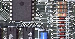
Printed circuit board
published: 2014-05-20
A printed circuit board (PCB) mechanically supports and electrically connects electronic components using conductive tracks, pads and other features etched from copper sheets laminated onto a non-conductive substrate. PCBs can be single sided (one copper layer), double sided (two copper layers) or multi-layer. Conductors on different layers are connected with plated-through holes called vias. Advanced PCBs may contain components - capacitors, resistors or active devices - embedded in the substrate.
Printed circuit boards are used in all but the simplest electronic products. Alternatives to PCBs include wire wrap and point-to-point construction. PCBs require the additional design effort to lay out the circuit but manufacturing and assembly can be automated. Manufacturing circuits with PCBs is cheaper and faster than with other wiring methods as component are mounted and wired with one single part. Furthermore, operator wiring errors are eliminated.
When the board has only copper connections and no embedded components it is more correctly called a printed wiring board (PWB) oretched wiring board. Although more accurate, the term printed wiring board has fallen into disuse. A PCB populated with electronic components is called a printed circuit assembly (PCA), printed circuit board assembly or PCB assembly (PCBA). The IPC preferred term for assembled boards is circuit card assembly (CCA),[1] for assembled backplanes it is backplane assemblies. The term PCB is used informally both for bare and assembled boards.
The world market for bare PCBs reached nearly $60 billion in 2012.[2]


