Search the entire web site and product database
Search the entire web site and product database
Tel:+86-0755-23724206
Fax:Please scan & email
E-mail:sales@hiquality-pcb.com
Contact:Shawn Wang

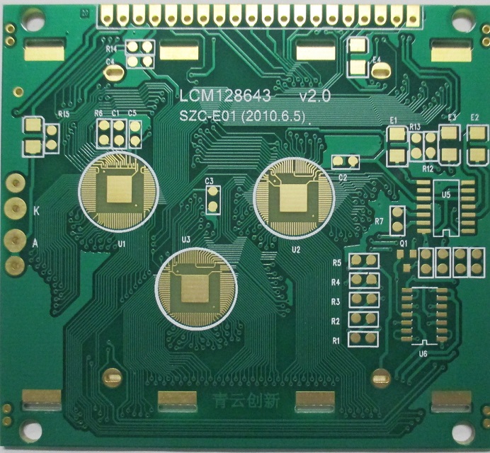
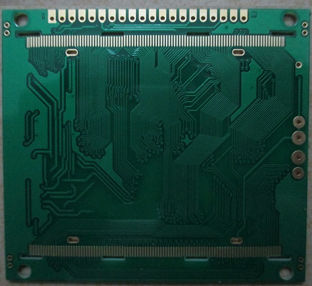
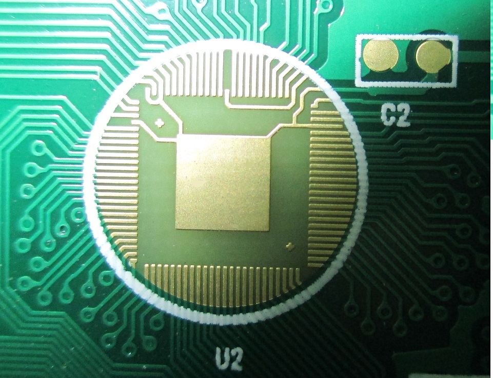
| Model:E0214040095A |
| Layers:2 layer |
| Thickness: 1.6mm |
| Hole Size: 0.2mm |
| Width/Space: 4mil |
| Surface Treatment: ENEPIG |

|
1 Hours promptly Quote 4 Hours promptly Engineering 24 Hours for 2 layer 2-5 Days for 4-20 layer 6-10 Days for 22+ layers 7*24 Hours online customer service |
Flexible PCB up to 12 layer Rigid Circuit Boards up to 48 layer Rigid-Flex Circuit Boards up to 36 layer Metal core printed circuit board 1-6 W/MK High Density(HDI)Circuit Boards(Max 4 ranks) |
Plant 1 add: Shenzhen, Guangdong, China Plant 2 add: Zhuhai, Guangdong, China Tel: +86-755-23724206 Email:sales@hiquality-pcb.com |
Copyright © 2014 All Rights Reserved.
High Quality PCB Co.,Limited